CETC Tier-1 distributor Jarwey|1200V SiC G2 vs G3: WM2HA020120L is not the 80 mΩ WM3HA080120L
The overview sheet calls G3 a high-frequency, low-RDS(on) planar generation. That label does not make WM3HA080120L the lower-resistance copy of WM2HA020120L. Version 3.0 prints 80 mΩ and 33 A on the G3 part, and 20 mΩ and 100 A on the G2 part. Both covers still say 1200 V and TO-247-4.
Whether the bus should be 650 V or 1200 V is already in the voltage-class note. The L/K/N pin split for the 20 mΩ family is in the suffix note. This page only separates the WM2HA prefix from the WM3HA prefix once 1200 V is already chosen.
Jarwey is a tier-1 distributor of SiC power devices from CETC Guiji Nanfang (55th Institute). CETC is the group mark. Guiji Nanfang is the unit under that group.
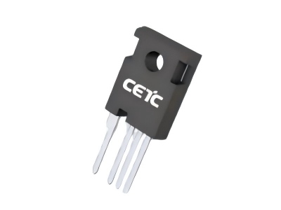
Read each resistance row at its own current
| Part | Generation / package | RDS(on) | ID / PD / RθJC | QG | Page |
|---|---|---|---|---|---|
| WM2HA020120L | G2 · TO-247-4 | 20 mΩ typ, 27.4 mΩ max VGS=18 V, ID=60 A 30 mΩ typ at 175°C | 100 A at 25°C, 79 A at 100°C (VGS=18 V) PD 517 W (case 25°C, junction 175°C) RθJC 0.29 °C/W typ | 217 nC typ VDS=800 V, VGS=−5/18 V, ID=32 A | 4 |
| WM3HA080120L | G3 · TO-247-4 | 80 mΩ typ, 96 mΩ max VGS=18 V, ID=15 A 130 mΩ typ at 175°C | 33 A at 25°C, 23 A at 100°C (VGS=18 V) PD 132 W (case 25°C, junction 175°C) RθJC 1.13 °C/W typ | 53.4 nC typ VDS=800 V, VGS=−5/18 V, ID=15 A | 614 |
| WM3HA080120K | G3 · TO-247-3 | Same 80 mΩ / 96 mΩ row VGS=18 V, ID=15 A 130 mΩ typ at 175°C | 33 A at 25°C, 23 A at 100°C PD 132 W, pulsed 76 A RθJC 1.13 °C/W typ | 53.4 nC typ at ID=15 A | 1027 |
All three list VDS = 1200 V. Absolute gate limits are −10 / +23 V. The recommended operating point on each Version 3.0 is −5 / +18 V. Threshold windows sit near 2.0–4.0 V, but the G2 test current is 20 mA and the G3 test current is 5 mA.
The 80 mΩ device is a 33 A switch
Conduction loss estimated at 100 A continuous and 20 mΩ does not survive a swap to 33 A and 80 mΩ. Junction-to-case thermal resistance moves from 0.29 °C/W to 1.13 °C/W, and the dissipation line moves from 517 W to 132 W under the same case/junction temperatures. Treat the G3 row as its own current class.
The two L datasheets list the same cover applications: renewable energy, EV battery chargers, high-voltage DC/DC, and switch-mode supplies. The overview maps G2 toward OBC, DC-DC, PV, and charging modules, and G3 toward DC-DC, server and datacenter supplies, and motor drives. Matching cover lines are not a ban on PV for the G3 part. Sort by the 100 A row versus the 33 A row first.
Do not divide 217 nC by 53.4 nC
Both gate-charge rows use VDS=800 V and VGS=−5/18 V. Drain current in the test is 32 A on the G2 part and 15 A on the G3 part. A driver peak scaled by 217/53.4 folds that current difference into a generation ratio. Recheck gate resistance against each switching-energy condition.
Stay on −5 V off and +18 V on. The overview also notes +15/−4 V as a compatible swing for G2 and G3. That swing is not the 15 V / 0 V feature line used on TO-252 flyback parts such as WM3HA160065E. Leave that line on the flyback thermal note.
The K suffix is the 3-lead 80 mΩ part
WM3HA080120K carries the same 80 mΩ table in TO-247-3. Its own application lines are EV motor drive, high-voltage DC/DC, and switched-mode supplies. Do not paste the 20 mΩ L/K pin essay onto this footprint. Read this datasheet’s package drawing. Nothing on the sheet authorizes an unverified swap.
Trench G4 in the overview sits on EV traction inverters. These two devices are planar G2 and G3. Ask Jarwey for a stocked G4 part number rather than inventing one here.
Seven checks before layout
- The bus is already 1200 V. This table is not the 650 V versus 1200 V split.
- Put either 100 A (25°C) or 33 A (25°C) into the loss equation. Do not drop 80 mΩ into a 20 mΩ conduction budget.
- Read RDS(on) at its own current: 18 V / 60 A for G2, 18 V / 15 A for G3, and keep the 175°C row separate.
- Keep 0.29 °C/W and 1.13 °C/W on different heatsink budgets.
- Compare QG only after writing down ID. Do not scale driver peak from 217 nC versus 53.4 nC alone.
- Design the gate for −5 / +18 V, inside −10 / +23 V absolute. Do not copy the WM3HA160065E 15 V / 0 V line.
- A TO-247-3 footprint points at WM3HA080120K and that drawing, not at the 20 mΩ pin note. Confirm the datasheet revision and samples with Jarwey.
Datasheets and product pages
Equivalent-spec wafer die available for order.
Related Articles